iPhone Motherboard Test Fixture Guide: Middle-Layer Repair
17 November 2026 · LightspeedTools team
Short answer: An iPhone motherboard test fixture is a socket that holds the two layers of a stacked logic board together through spring contacts, so you can power up and test the board without soldering the layers back together. Separate the layers on a preheater, test each one in the fixture to find which layer holds the fault, repair it, and only rejoin the board with a reballed interposer once the fixture shows it working.
Stacked logic boards changed board-level iPhone repair. A fault that used to be found with a multimeter on one flat board can now sit on either of two layers, or in the hundreds of solder joints between them. A layered test fixture turns that guesswork into a simple swap-and-test process. This guide covers how the boards are built, when and how to separate them, how to test each layer and how to rejoin them without creating a new fault.
What a stacked (sandwich) logic board is
From about the iPhone X generation onward, Apple moved from a single flat logic board to a stacked design: two boards placed on top of each other and joined by an interposer, a thin frame-shaped board with solder balls on both faces. The interposer carries power, signals and ground between the two layers and holds them a fixed distance apart, which lets components sit on the inner faces of both boards.
The split of components differs by model, but on many generations one layer carries the processor, storage and most of the power management, while the other carries much of the cellular and RF section. Treat that as a rough guide only. Before you work on a specific model, check its schematic or board view to see exactly what sits on each layer.
The stacked design saves space for a bigger battery. For the technician it means three places a fault can hide: the upper layer, the lower layer and the interposer joints.
Why separate the layers
- Fault isolation. Testing each layer against a known-good partner in a fixture shows whether the fault is on the CPU side, the RF side or in the joints between them.
- Access to components. Many parts sit on the inner faces of the sandwich. You cannot measure, reflow or replace them while the board is joined.
- CPU and NAND work. Reballing or replacing the processor or storage chip needs the layer on its own, flat and supported.
- Interposer faults. Cracked joints after a drop can only be repaired by separating, cleaning and reballing.
Separation is not a first step. Run the usual checks first: current draw on a power supply, diode-mode readings on the main lines and a close look under a microscope. Our guide to board-level diagnosis of a phone that will not turn on covers that groundwork. Separate only when those checks point inside the sandwich or to a component you cannot reach.
What a layered test fixture does
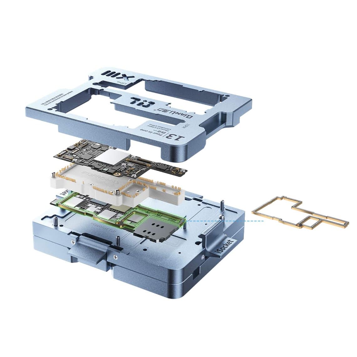
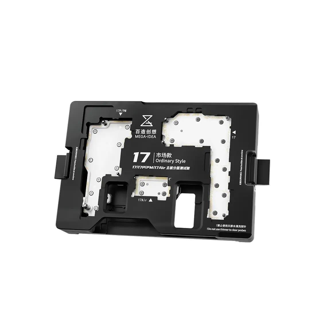
A layered test fixture replaces the soldered interposer with a spring-pin or contact socket. You place the upper and lower layers in the fixture, close it, and the pins connect the two boards the way the interposer would. Most fixtures also break out connectors so you can attach the battery, display and other flex cables, or a power supply, and boot the board on the bench.
Fixtures are model-specific because the interposer shape and pad layout change between generations. Examples on our shelves include:
- iPhone X and XS: the JC TX-BAS / TX-PRO double-layer fixture and the Fix-XS iSocket 2-in-1.
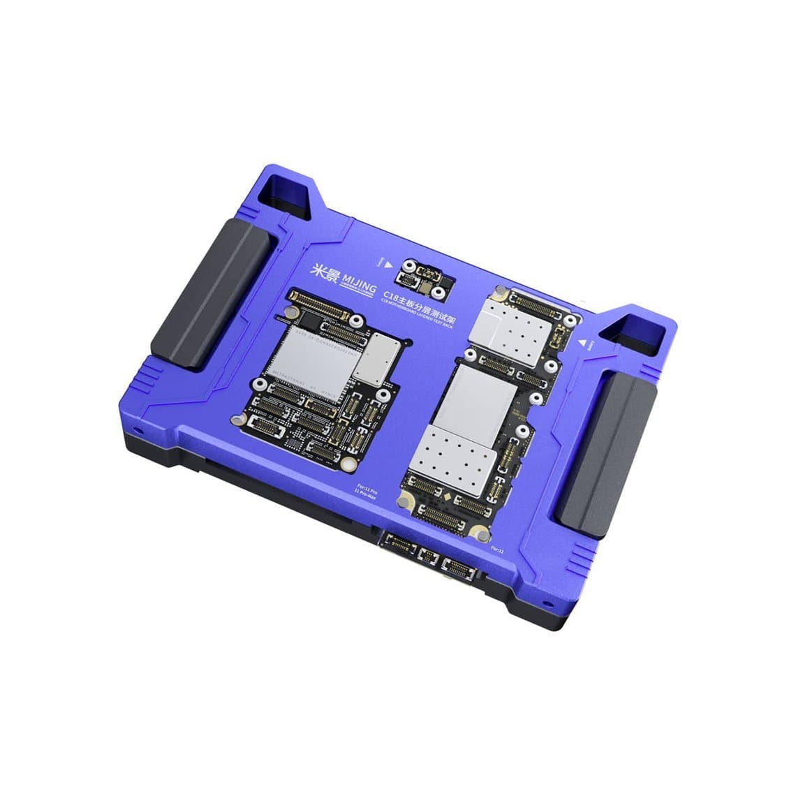
- iPhone 11 series: the Mijing C18.
- iPhone 13 series: the Qianli 4-in-1 layered fixture.
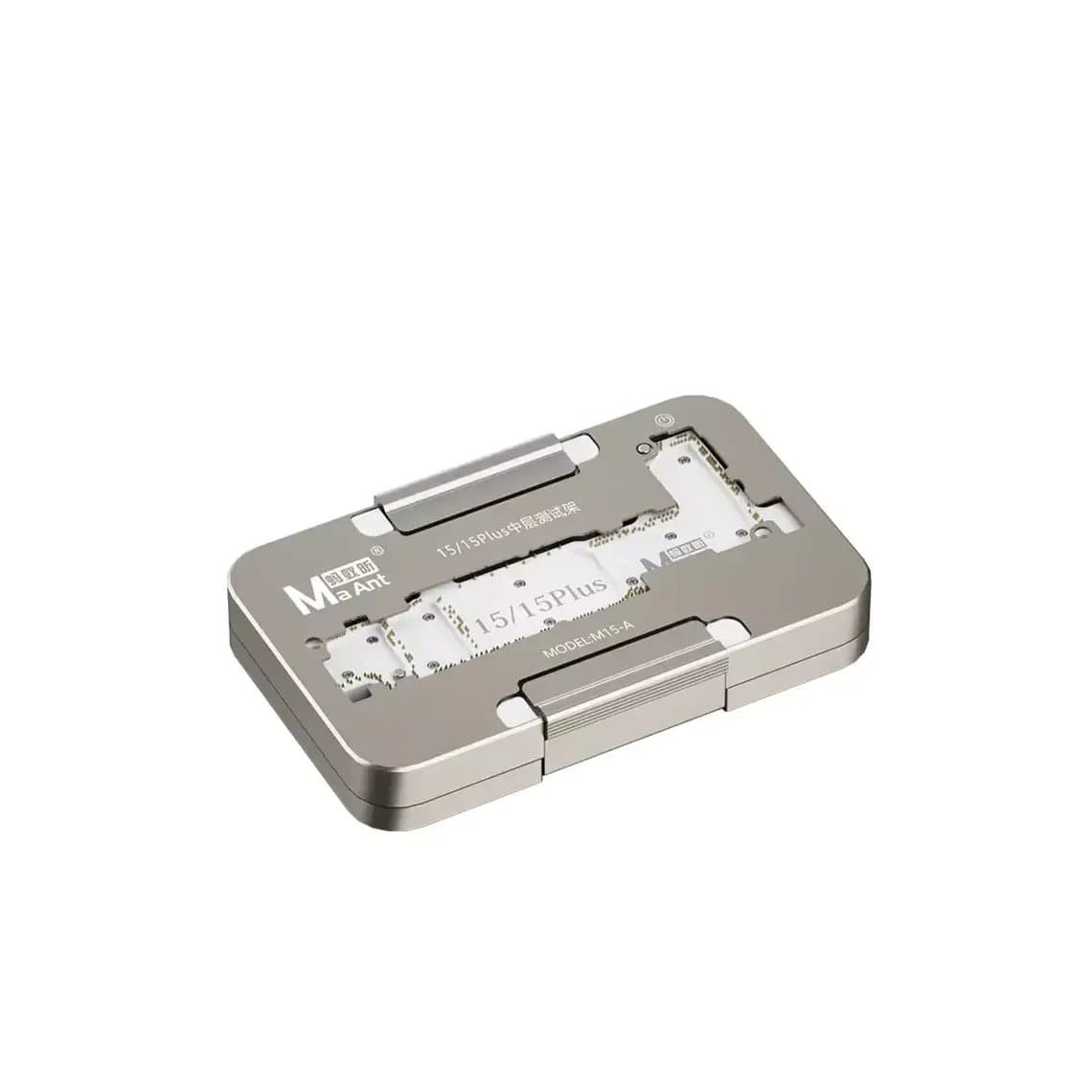
- iPhone 15 series: the MaAnt M15 and the Mijing C23.
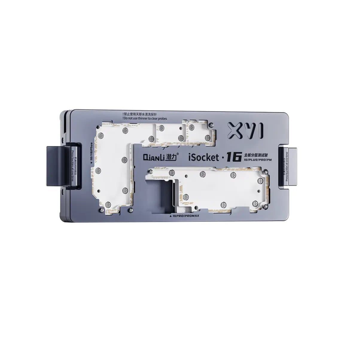
- iPhone 16 and 17 series: the Qianli iSocket for iPhone 16 and the Mega-Idea 4-in-1 for iPhone 17.
The full range by model is in our PCB test fixtures category. Check the exact model coverage before you buy, as fixtures that cover a "series" do not always cover every variant.
Step-by-step: separate, test, repair, rejoin
1. Prepare the board
Remove the board from the phone, take off any removable shields and parts that could fall or shift, and note the condition of the board under a microscope. Photograph both sides. Work on an ESD-safe mat with a grounded strap.
2. Separate on a preheater or separation platform
Clamp the board in a holder over a PCB preheater or a dedicated separation platform. The bottom heat brings the whole board up evenly so the top heat does not have to do all the work, which reduces warping and stress on the chips.
- Apply flux around the interposer edges.
- Bring the board up gradually, then add hot air evenly around the interposer, not on one spot.
- Lift the upper layer only when the solder has fully melted. If it resists, it is not ready. Prying cracks pads and tears traces.
There is no single correct temperature. It depends on the model, the solder used at the factory, any low-melt solder from a previous repair, the platform and your hot-air station. Follow the platform maker's guidance and the profile used by experienced technicians for that exact board, and practise on scrap boards first.
3. Clean the pads
Let the layers cool on their own. Clean the pads on both boards and the interposer with flux and solder wick, using light pressure so you do not lift pads. Inspect every pad under the microscope; a missing or torn pad needs a jumper before the board goes any further.
4. Test each layer in the fixture
Seat both layers in the fixture and connect a DC power supply or battery. Watch the current draw as the board starts. Then work through the symptom: boot, display, charging, service, Wi-Fi, audio, cameras.
If you have a known-good layer from a donor board of the same model, swap one layer at a time. If the fault follows a layer, it lives on that layer. If both layers test good in the fixture but the joined board failed, the interposer joints were the problem.
Keep pairing in mind. Some components on the processor side are tied to each other and to the phone, so a donor layer is a diagnostic tool first. Do not assume a permanent layer swap will keep every function working.
5. Repair the faulty layer
With the faulty layer isolated, repair it as you would any board: measure, replace components, reball chips. Retest in the fixture after each repair, before any rejoining.
6. Reball the interposer
Use a stencil made for that model's interposer, fitted with solder paste, to put a fresh, even set of balls on the interposer or the board pads. Our BGA reballing stencils include interposer stencils for many iPhone generations. The technique is the same as chip reballing, covered step by step in how to reball a BGA chip. Many technicians use a lower-melting paste for the interposer so later separation and rejoining stress the board less; whatever you use, use it consistently and know its melting range.
7. Rejoin and retest
Align the layers carefully, using the board's alignment features or the platform's guides, and reflow them back together on the preheater. Let the board cool, then test it in the phone. A board that worked in the fixture but fails after rejoining usually has an open or bridged interposer joint.
Common failure points
| Failure point | Typical cause | What you may see |
|---|---|---|
| Cracked interposer joints | Drops, bending, repeated heat cycles | Intermittent faults that change when the board is pressed; no service, no boot or missing functions |
| Lifted or torn interposer pads | Prying before the solder melted, rough pad cleaning | Open lines after rejoining; needs jumpers |
| Short on one layer | Liquid damage, failed capacitor, power faults | High current draw in the fixture with that layer fitted |
| Heat damage to chips | Too much or uneven heat during separation | New faults on CPU or storage after the repair |
Risks and how to reduce them
- Overheating. Processor, storage and the underfill around them can be damaged by long or uneven heating. Use bottom heat, even top heat and the shortest time that works.
- Board warping. Uneven heat bends layers, so the interposer will not seat flat on rejoining. Support the board fully on the platform.
- Data loss. Any board-level work on the storage side can end in lost data. Tell the customer before you start.
- Pairing. Swapping processor-side parts or layers between phones can disable features tied to the original parts.
- Repeated cycles. Each separation stresses pads. Test thoroughly in the fixture so you only rejoin once.
- Lithium safety. Remove the board from the phone before heating, and keep batteries well away from the preheater.
Questions
Which iPhones have a stacked logic board?
Stacked, two-layer logic boards appear from about the iPhone X generation onward, and later flagship models have kept the design. The layout of each layer and the interposer changes between generations, which is why test fixtures and stencils are model-specific.
Can I test an iPhone board without soldering the layers back?
Yes, that is what a layered test fixture is for. It connects the two layers through spring contacts so you can power up and test the board, then rejoin it only once you know it works.
What temperature separates an iPhone motherboard?
There is no universal figure. It depends on the model, the solder, any previous repair, and your preheater and hot-air station. Follow the equipment maker's guidance and practise on scrap boards before working on a customer board.
Is the interposer the same as the two boards?
No. The interposer is the thin frame-shaped board between the two layers that connects them. It is often where drop damage shows up, as cracked solder joints that cause intermittent faults.
A good fixture pays for itself the first time it shows which layer holds the fault. Browse our motherboard test fixtures by model, all checked before they ship from Shenzhen. Repair shops can unlock wholesale pricing and reorder fixtures, stencils and paste by SKU through Quick Order.